|
|
|

Optomec is a privately-held, rapidly growing supplier of Additive Manufacturing systems.The Company's patented 2D and 3D printing technologies work with the broadest spectrum of functional "inks", including all variety of electronic materials, high performance metals and even biological matter. Optomec has more than 150 marquee customers around the world, targeting production applications in the Electronics, Energy, Life Sciences and Aerospace industries.
Optomec LENS����ֱ�ӽ�������(����)
Optomec��ӯ����,�������������Ĺ�˾������ͻ����������������������һ���ڵ��ӡ���Դ��������ѧ������/�������졣
Optomec��һ�����ϵļӷ����������(��ijЩ����±���Ϊ��3Dӡˢ��)һ�������Եķ���,�Ѿ���֤ʵ�ڽ��ͳɱ�����߹���,��������ʱ����о������ơ��ù�˾��Ͷ���˳���3000����Ԫ�Ŀ����������,��Խ��ǰ��������������ҪӦ������������ٹ�ģ�ͳɱ��ĵ����豸,���Ч�ʵ�һ���������Դ,�ӳ������ĸ�ֵ�ĺ����㲿��,������ĥ��ҽ���豸��
����ҵ��Optomec�ӷ�����ϵͳ����1997��,������15������150����װϵͳ�Ŀͻ���վ�����ǵĿͻ�Ⱥ����������������ҵ����ʹ��Optomecϵͳ����δ���������Ʒ,������Ҫ�������ֻ���̫���ܺʹ�������ʾ�������̡�ʵ���Һ�������֯������ҿ�������Դʵ����(NREL),���Ͷ�����,NASA,ɣ���ǹ���ʵ����,�Լ������վ�,����½������������,ͬ��ʹ��ϵͳ������һϵ�е���ҵ�;���Ӧ�á�һ��ȫ��ѧ����������������������ѧ����ʢ�ٴ�ѧ����Ϧ������������ѧ��ŦԼ������ѧ,��������ʿ��ѧ(�Ĵ�����),POSTECH(����),Sinano(�й�),�и�������ڿ�����һ���Ĺ���ʦ�Ϳ�ѧ�ҵ���༼��Optomec�ӷ����켼����
Optomec��һ��˽�˿عɹ�˾,�ܲ���������ī�����ݰ��������ˡ���˾ӵ���ֳ����ۺ�֧�ְ��´��鲼����,��һ��ȫ������ľ����̺ʹ����̡��ù�˾�������Ʒ��ȫ��oem��ϵͳ�����̺����û���һ�����������г���Optomec���д���֪ʶ��Ȩ�ʲ�,����������ʮ�������˺�������ʮ���ȴ��е�,��������ļӷ����졣
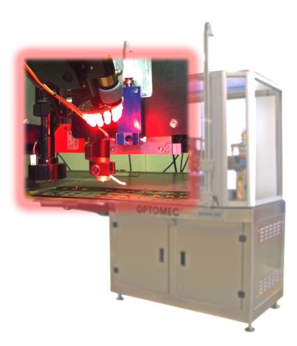
Aerosol Jet Lab Systems
Aerosol Jet Lab systems are ideally suited to develop next generation processes and devices for photovoltaic, touch screen displays, 3D interconnects and other printed electronics and biologics applications. A number of Aerosol Jet Lab system configurations are available to meet your specific application requirements.
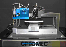
Aerosol Jet 300 Systems
Key Features
- Work area 300mm x 300mm
- 300mm XY motion Control System
- Atomizers
- 2 Pneumatic (model 2P) or
- 2 Ultrasonic (model 2U) or
- 1 Ultrasonic & 1 Pneumatic (model UP)
- Dual Atomizer Deposition Control Systems
- Fine Feature Deposition Head with Heater & Shutter
- Heated Platen
- Stainless Steel Cabinet with Granite Table Top
- Safety Enclosure (CE)
- Optional 700 mW Laser or UV Cure Systems
- Optional Wide Feature Deposition Head
Applications
Workhorse platform for general material science R&D and low-volume fabrication of electronic circuitry and components. Also ideal for product development, prototyping and life sciences research. Example applications include:
- 3D Interconnects for multi-chip packages
- Embedded passives
- Printed sensors and antennas on conformal surfaces
- Bio fabrication
Print Capabilities
- Fine Feature sizes to 10 um
- Wide Features Sizes to 1 cm
- Thin layer deposits from 100 nm
- Many inks and substrates
- Ink viscosity range from 1-1000 cP
- Nano material deposition
- Planar and Non-Planar Capabilities
- Low Temperature Processing
Aerosol Jet Dispense System Configurations
Standard Features
- AJMD 300 - Work area 300mm x 300mm
- AJMD 470 - Work area 470mm X 370mm
- +/-6 microns accuracy, +/- 2 microns repeatability XY motion
- Atomizers: 1 Ultrasonic & 1 Pneumatic
- Dual Atomizer Deposition Control Systems
- Interchangeable Fine and Wide Feature
- Deposition Head with Shutters
- Heated Platen
- Stainless Steel Cabinet with Granite Table
- Safety Enclosure (CE)
- Advanced vision and lighting controls
- Programmable dispense recipes
Optional Features
- 700 mW Laser
- UV Cure Systems
- Wide Feature Deposition Head with integrated shutter
Applications
Batch platform for R&D and low-volume manufacturing of electronic circuitry and components. Example applications include:
- Component / Die Attach
- Component Underfill and Encapsulation
- 3D Interconnects for Stacked Die & Other
- Complex Packaging Applications
- Embedded Passives
- Small Footprint Packaging
- Repair & Re-Work of Production Defects
- Cost Effective Low Volume Manufacturing
Print Capabilities
- Fine Feature sizes to 10 um
- Wide Features Sizes to 1 cm
- Thin layer deposits from 100 nm
- Many inks and substrates
- Ink viscosity range from 1-1000 cP
- Metal, epoxy and other material depositions
- Planar and Non-Planar Capabilities
- Low Temperature Processing
����Ʒ�ڹ������ж�ҿͻ��������Ҫ�ιۻ��˽�����ʹ��״������Ͳ�ɫ��ϵ��
Optomec����˾���������������ڿ���һ���µ����ֻ�����������������ƶ��豸Ӧ�ó��������õ����ߣ�����ֱ�Ӵ�ӡ��
�ý�������ǻ���Optomec�����ܽ�����ӡˢ���Ӽ�����ƽ�����ά��3D�������ϴ�ӡ�������Ӽ����������ʹ�á�
��Optomec�����ܽ�����ӡˢ���������۽���ȷ�������ײ��ϣ�������ϸ�Ĺ��ܵ�·��Ƕ��ʽ������ɴ˲����Ĺ��ܵĵ��Ӳ�Ʒ�߿��Ⱥ�ͼ���Ĺ��ܣ���10�����ײ��ȡ��Ӷ����ͳɱ���
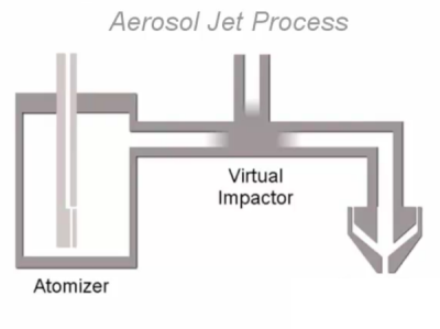
����������£����ܽ����似��������ֱ�Ӵ�ӡ���������ϵ�Ƭ�ͻ���ʹ������������ī�����ߡ�
ӡˢ�����о�ȷ�ؿ��ƿ�λ�ã�������״�ͺ�ȣ�������һ���⻬�ľ����ı�����ȣ���ȷ���������ܡ���ƻ���ʹ�ù����жԻ����к��IJ��ϡ�
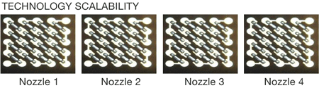
�ƶ��豸�����ߣ�����LTE��NFC��GPS��WIFI��WLAN��BT��ӡˢʹ�����ܽ�������̶����������ֻ��㲿����Ӧ�̡��������ߵ����������������������������ܽ�����ӡ�����տ���չ�� - �����߿��Դ�ӡ��4��ͬʱ��һ̨����������һ�����͵����߷���ͼ��������������300ƽ������ƽ��ÿ��30,000����
Optomec����άӡˢ���ߵĽ�������п������ŵؽ��ͳɱ����������ڸ�Ч�����Ӽ�������̵��ֳ��豸�������ȡ���Ҳ�Ի����ͽ����ĺô�����Ϊ����ȫ��������Ҫ���л�ѧ�ƺ��к�����������������Ŀǰ�����췽����
|

 ����CCD���˹�����