SiO2/Si基底CVD石墨烯,石墨烯套装,SiO2基底单层石墨烯,SiO2基底单/双层石墨烯 |
 |
CVD石墨烯:SiO2/Si基底
CVD Graphene on SiO2/Si
Graphene Film Trial Kit, 石墨烯套装
Monolayer Graphene on 285 nm SiO2 Wafer,
285nm SiO2基底单层石墨烯
Monolayer Graphene on 90 nm SiO2 Wafer,
90nm SiO2基底单层石墨烯"
Single/Double Layer Graphene on 285 nm Silicon Dioxide Wafer, 285nm SiO2基底单/双层石墨烯
Single/Double Layer Graphene on 90 nm Silicon Dioxide Wafer,
90nm SiO2基底单/双层石墨烯
CVD石墨烯:SiO2/Si基底 CVD Graphene on SiO2/Si |
|||
| Graphene Film Trial Kit 石墨烯膜套装 |
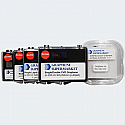 |
Includes: Two Single/Double Layer Graphene samples on 285 nm Silicon Dioxide Wafers: 1cm x 1 cm Two 10mmx10mm samples, Graphene Film on Nickel: 1 cm x 1 cm One sample of Multilayer Graphene on a 285 nm Silicon Dioxide Wafer: 1 cm x 1 cm One sample of Monolayer Graphene on a 285 nm Silicon Dioxide Wafer: 1 cm x 1 cm One sample of Monolayer Graphene on Glass: 1" x 1" If you are interested in investigating numerous different samples of graphene coatings, this trial kit is ideal. All of the samples are made by Chemical Vapor Deposition and give a strong Raman signal. A great value for students and scientific researchers alike interested in trying different samples. |
|
| Monolayer Graphene on 285 nm SiO2 Wafer 285nm SiO2基底单层石墨烯 |
4” (100mm) wafer | 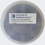 |
Monolayer graphene on silicon wafers (p-doped) with a 285 nanometer silicon dioxide coating. Properties of Graphene Film: The thickness and quality of our graphene films is controlled by Raman Spectroscopy The graphene coverage of this product is about 95% The graphene film is continuous, with occasional holes and cracks The graphene film is polycrystalline, i.e. it consists of grains with different crystallographic orientation Sheet Resistance: 660-1,500 Ω/□ Our graphene films are predominantly single-layer graphene (more than 97%) with occasional small multilayer islands. Properties of Silicon/Silicon Dioxide Wafers: Oxide Thickness: 285 nm Color: Violet Wafer thickness: 525 micron Resistivity: 0.001-0.005 ohm-cm Type/Dopant: P/Boron Orientation: <100> Front Surface: Polished Back Surface: Etched Our graphene films are manufactured using a PMMA assisted transfer method. 拉曼光谱图 / 光学图像 / 4” (100mm) wafer 尺寸图 |
| 10mm×10mm 10片 | 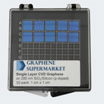 |
||
| 10mm×10mm 5片 |  |
||
| Monolayer Graphene on 90 nm SiO2 Wafer 90nm SiO2基底单层石墨烯 |
10mm×10mm 5片 | 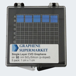 |
Monolayer graphene on silicon wafers with 90 nanometer silicon dioxide coating. Properties of Graphene Film: The thickness and quality of our graphene films is controlled by Raman Spectroscopy The graphene coverage of this product is about 95% The graphene film is continuous, with occasional holes and cracks The graphene film is polycrystalline, i.e. it consists of grains with different crystallographic orientation Sheet Resistance: 660-1,500 Ω/□ Our graphene films are predominantly single-layer graphene (more than 97%) with occasional small multilayer islands. Properties of Silicon/Silicon Dioxide Wafers: Oxide Thickness: 90 nm Color: Violet Wafer thickness: 525 micron Resistivity: 0.001-0.005 ohm-cm Type/Dopant: P/Boron Orientation: <100> Front Surface: Polished Back Surface: Etched Our graphene films are manufactured using a PMMA assisted transfer method. 拉曼光谱图 / 光学图像 |
| Single/Double Layer Graphene on 285 nm Silicon Dioxide Wafer 285nm SiO2基底单/双层石墨烯 |
10mm×10mm 10片 | |
Mono and bilayer graphene on silicon wafers (p-doped) with a 285 nanometer silicon dioxide coating. The samples have nearly full monolayer coverage with 10-30% coverage of bilayer graphene islands. They are a great low-cost alternative to monolayer graphene for select purposes. Properties of Graphene Film: The graphene coverage of this product is about 95% The graphene film is continuous, with occasional holes and cracks The graphene film is polycrystalline, i.e. it consists of grains with different crystallographic orientation Properties of Silicon/Silicon Dioxide Wafers: Oxide Thickness: 285 nm Color: Violet Wafer thickness: 525 micron Resistivity: 0.001-0.005 ohm-cm Type/Dopant: P/Boron Orientation: <100> Front Surface: Polished Back Surface: Etched Our graphene films are manufactured using a PMMA assisted transfer method. 光学图像 / 典型SEM图像 |
| Single/Double Layer Graphene on 90 nm Silicon Dioxide Wafer 90nm SiO2基底单/双层石墨烯 |
10mm×10mm 10片 | |
Mono and bilayer graphene on silicon wafers (p-doped) with a 90 nanometer silicon dioxide coating. The samples have nearly full monolayer coverage with 10-30% coverage of bilayer graphene islands. They are a great low-cost alternative to monolayer graphene for select purposes. Properties of Graphene Film: The graphene coverage of this product is about 95% The graphene film is continuous, with occasional holes and cracks The graphene film is polycrystalline, i.e. it consists of grains with different crystallographic orientation Properties of Silicon/Silicon Dioxide Wafers: Oxide Thickness: 90 nm Color: Violet Wafer thickness: 525 micron Resistivity: 0.001-0.005 ohm-cm Type/Dopant: P/Boron Orientation: <100> Front Surface: Polished Back Surface: Etched Our graphene films are manufactured using a PMMA assisted transfer method. 光学图像 / 典型SEM图像 |
|
上海玻色智能科技有限公司 上海: (021)3353-0926, 3353-0928 北京: (010)8217-0506 广州: 139-0221-4841 武汉: 139-1733-4172 全国销售服务热线:4006-171751 Email: info@bosontech.com.cn www.BosonTech.com.cn 2008-2022 All Rights Reserved! |
|