CVD石墨烯,镍箔基多层石墨烯,镍基石墨烯,铜箔基单层石墨烯,铜箔基单层/双层石墨烯 |
 |
CVD石墨烯:金属基
CVD Graphene on Metals
Multilayer CVD Graphene on Nickel foil,镍箔基多层石墨烯
CVD Graphene Film on Nickel,镍基石墨烯
Single Layer CVD Graphene on Copper foil,铜箔基单层石墨烯
Single/Double Layer CVD Graphene on Copper Foil,铜箔基单层/双层石墨烯
CVD石墨烯:金属基 CVD Graphene on Metals |
|||
| Multilayer CVD Graphene on Nickel foil 镍箔基多层石墨烯 |
2”×2” | 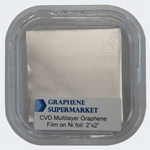 |
Nickel foil thickness: 25 micron We offer multilayer graphene films that are about 300 monolayers (105 nm) thick on average. These graphene films are grown on nickel foil and continuous across nickel surface steps and grain boundaries. The graphene grown on nickel film is multilayer and is not uniform. It looks like a patchwork whereas the “patches” have different thicknesses. The graphene layers within the same patch are aligned relative to each other (there is a graphitic AB-staking order). The size of the patches is about 3-10 microns. 典型SEM图像 / 转移到玻璃基底以后的透过率曲线 |
| CVD Graphene Film on Nickel 镍基石墨烯 |
4” (100mm) wafer | 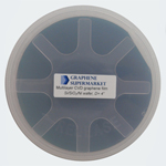 |
Graphene on nickel is a few monolayers thick, usually between 1-7 layers with an average of 4 monolayer thickness. It looks like a patchwork, whereas each “patch” has a different thickness. The graphene layers within the same patch are aligned relative to each other (there is a graphitic AB-stacking order). The size of each patch is about 3-10 microns. Because graphene on nickel is grown in patches with different layering, the Raman signal will change dramatically depending on the spot of the film where it is taken. If nickel is used as a catalyst, it is not possible to create a graphene sheet with a precise and uniform layering. 典型SEM图像 / 光学图像 |
| 10mm×10mm 10片 | 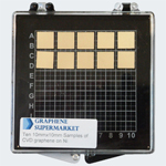 |
||
| 10mm×10mm 20片 | 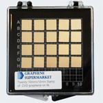 |
||
| Single Layer CVD Graphene on Copper foil 铜箔基单层石墨烯 |
2”×2” | 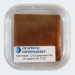 |
Copper foil thickness: 20 micron We offer graphene films that are predominantly single-layer graphene. These graphene films are grown on copper foil and continuous across copper surface steps and grain boundaries. Graphene is grown on both sides of the copper foil. If you require specifically graphene on one side only, please contact us directly. Etching of the underlying copper foil allows the carbon films to be transferred to other substrates such as glass, silicon dioxide or plastic films. To the best of our knowledge, there is no report of degradation of the CVD graphene over time when it is kept in a safe, dry place. The copper foil with single-layer graphene can exhibit some coloration due to slow oxidation of the copper foil, which does not affect the quality of the graphene film. 典型SEM图像 |
| 4”×2” | 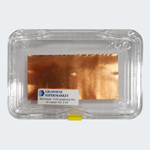 |
||
| 4”×4” | 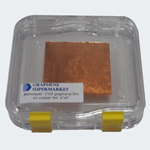 |
||
| Single/Double Layer CVD Graphene on Copper Foil 铜箔基单层/双层石墨烯 |
4”×2” | 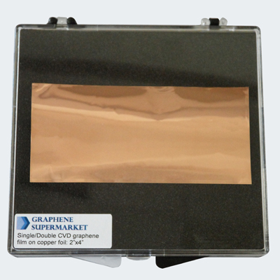 |
Copper Foil is 20 Microns Thick The graphene film is mostly monolayer and has 10%-30% bilayer islands Single/double layer graphene is a cost-effective alternative to monolayer graphene on Cu foil. These graphene films are grown on copper foil and continuous across copper surface steps and grain boundaries. Graphene is grown on both sides of the copper foil. If you require specifically graphene on one side only, please contact us directly. Etching of the underlying copper foil allows the carbon films to be transferred to other substrates such as glass, silicon dioxide or plastic films. To the best of our knowledge, there is no report of degradation of the CVD graphene over time when it is kept in a safe, dry place. The copper foil with single/double layer graphene can exhibit some coloration due to slow oxidation of the copper foil, which does not affect the quality of the graphene film. 典型SEM图像1 / 典型SEM图像2 |
|
上海玻色智能科技有限公司 上海: (021)3353-0926, 3353-0928 北京: (010)8217-0506 广州: 139-0221-4841 武汉: 139-1733-4172 全国销售服务热线:4006-171751 Email: info@bosontech.com.cn www.BosonTech.com.cn 2008-2022 All Rights Reserved! |
|