导电薄膜基底CVD石墨烯,PET基单层石墨烯,PET基单壁碳纳米管,石英基单层石墨烯,玻璃基单层石墨烯 |
 |
CVD石墨烯:导电薄膜基底
CVD Graphene on Conductive Coatings
Monolayer Graphene on PET,
PET基单层石墨烯
Single Walled Carbon Nanotubes on PET,
PET基单壁碳纳米管
Monolayer Graphene film on Quartz, 石英基单层石墨烯
Monolayer Graphene on Glass,
玻璃基单层石墨烯
CVD石墨烯:导电薄膜基底 CVD Graphene on Conductive Coatings |
|||
| Monolayer Graphene on PET PET基单层石墨烯 |
1” ×1” | 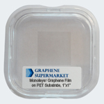 |
Monolayer graphene film is grown by CVD processing onto copper foil, then transferred onto PET (Polyethylene terephthalate) Properties of Graphene Film on PET: The graphene coverage is about 95% The graphene film is continuous, with occasional holes and cracks The graphene film is polycrystalline, i.e. it consists of grains with different crystallographic orientation Sheet resistance 660-1500 Ω/□ PET Thickness: 7 mil=175 micron Please note that it is difficult to obtain a Raman spectrum of graphene film directly on PET due to a strong background signal. We can manufacture custom, large-size coatings, and use different shapes and types of plastic materials. You may also send us your own substrates for coating. Few-layer graphene coatings with a lower sheet resistance and lower transparency can also be prepared. Please contact us for a quote. Our graphene films are made by a PMMA assisted transfer method. |
| 1” ×1” 5片 | |
||
| 2” ×2” | 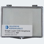 |
||
| Single Walled Carbon Nanotubes on PET PET基单壁碳纳米管 |
1” ×1” |  |
Single-Walled Carbon Nanotube Coatings Specifications: Transparency: 83%~90% at 550 nm wavelength Sheet Resistance: 600~1800 Ω/□ PET Thickness: 7 mil=175 micron 透过率曲线 / 典型SEM图像1 / 典型SEM图像2 |
| 1” ×1” 5片 | |
||
| Monolayer Graphene film on Quartz 石英基单层石墨烯 |
1” ×1” |  |
Monolayer graphene film is grown by CVD processing onto copper foil, then transferred onto quartz Properties of Graphene Film on Quartz: The thickness and quality of graphene films is controlled by Raman Spectroscopy The graphene coverage of this product is about 95% The graphene film is continuous, with occasional holes and cracks The graphene film is polycrystalline, i.e. it consists of grains with different crystallographic orientation The transmission of our graphene film is above 97% Sheet Resistance: 660-1,500 Ω/□ Properties of Quartz Substrate: We use G.E. 124 Fused Quartz Substrates Knoop Hardness: >600 Kg/mm2 Density: 2.21 g/cm3 拉曼光谱图 |
| 1” ×1” 5片 |  |
||
| Monolayer Graphene on Glass 玻璃基单层石墨烯 |
1” ×1” 5片 |  |
Monolayer graphene film is grown by CVD processing onto copper foil, then transferred onto glass Properties of Graphene Film on Glass: The thickness and quality of graphene films is controlled by Raman Spectroscopy The graphene coverage of this product is about 95% The graphene film is continuous, with occasional holes and cracks The graphene film is polycrystalline, i.e. it consists of grains with different crystallographic orientation The transmission of our graphene film is above 97% Sheet Resistance: 660-1,500 Ω/□ Properties of Glass Substrate: We use Corning EAGLE XGTM AMLCD Glass Substrates Thickness: 0.7 mm Density: 2.38 g/cc 拉曼光谱图 |
| 2” ×2” | 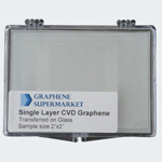 |
||
|
上海玻色智能科技有限公司 上海: (021)3353-0926, 3353-0928 北京: (010)8217-0506 广州: 139-0221-4841 武汉: 139-1733-4172 全国销售服务热线:4006-171751 Email: info@bosontech.com.cn www.BosonTech.com.cn 2008-2022 All Rights Reserved! |
|